
I wanted to have a modern storage solution for my 6502 homebrew computer and that naturally leads to SD cards. The easiest way to interact with an SD card is probably in SPI mode, with the added benefit that you can later add more SPI devices. The web is full of intros to the SPI protocol, incl. https://www.circuitbasics.com/basics-of-the-spi-communication-protocol/
In short we will need a clock line (CLK), serial out (MOSI), serial in (MISO), and a “Slave Select” (SS) line for each device. At least for now I chose to set it up so I can have 3 slave devices connected to the SPI port, controlled by PB2-PB4 on the VIA.
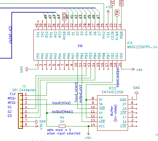
The most important design decision was to use the VIA timer to create the SPI clock signal. The T2 timer can create a clock signal that is output on CB1 and the frequency is PHI2 / (2*(N+2), where N is the value you set T2 to count down from (and PHI2 the system clock). Choosing N = 0 the SPI clock becomes 1/4 of the system clock or e.g. 250 kHz if you are using a 1MHz clock for the 6502.
Most other solutions I could find on the web manually created a clock signal by the 6502 writing directly to the VIA. Two writes to set the clock high/low and one read for each bit is at least 12 clock cycles, so the max frequency using this method is 1/12th the system clock frequency. Using T2 (and the VIA’s shift register) we should get at least 3X the speed.
The other advantage is that T2 can be set up to control the VIA’s shift register with bits being sent or received on CB2 and as such the 6502 processor does not have to read every single bit; it can just e.g. read a full byte once the shift register is full. This further increases speed of communications, rather than having the 6502 read and shift every bit.
However there is only one shift register (that can be set to either send or receive) and the SPI protocol calls for separate lines for sending and receiving bits. So I chose to add a buffer to switch between MOSI and MISO being routed to CB2 on the VIA. I use PB1 and PB2 to set which of the lines are enabled on the buffer – and I have pulled MOSI high when the output on the buffer is disabled. This works since – at least for the SD card – there is no simultaneous sending and receiving of bits.
I could of course reduce that to only using one pin on the VIA to control output (MOSI) or input (MISO) by adding a not-gate, but at least from now have not added the extra chip. If I need more glue logic for something else later I certainly will change this (it does annoy me a little to “waste” a pin on the VIA that could be used for something else).
Hopefully this helps explain the HW setup of the SPI interface and in my next blog post I will describe the code for implementing the SPI protocol.
One Reply to “SPI part 1”